TEM CN STU group:
Mária Čaplovičová, Viliam Vretenár, Mário Kotlár
The Head of TEM CN STU group is Mária Čaplovičová. She has a long-lasting and broad experience in Transmission Electron Microscopy (TEM), High Resolution TEM (HRTEM), Selected Area Electron Diffraction (SAED), Energy Dispersive X-ray Spectroscopy (EDX), and Scanning Electron Microscopy (SEM) techniques and in application of all these methods to characterization of inorganic natural and synthesized nanostructures and other materials.
Infrastructure of CN STU
The Centre is equipped with an state-off the -art double corrected analytical transmission electron microscope with an atomic resolution JEM-ARM200cF from JEOL company. The microscope is equipped with a cold field emission cathode – cFEG with an energy resolution of < 0.35eV @ 200 kV. STEM and TEM spherical aberration correctors allow resolutions of 78 pm in STEM mode and of 110 pm in TEM mode. It works in TEM (cTEM, HRTEM, ARTEM) and STEM (STEM-BF, STEM- ABF, STEM-HAADF STEM-LAADF, SEI/BEI) image modes. Sample structural information can be obtained using electron diffraction methods (selected area (SAED), precession (PD), convergent beam (CBD), nanobeam (NBD) diffractions. The microscope allows to determine the elemental composition using EDS and EELS methods at atomic level. Moreover, it also allows the holography imaging, electron tomography imaging, and orientation mapping using ASTAR software.
There is also an older Transmission Electron Microscope Jeol JEM 2000FX for a routine work.
JEM ARM 200cF is equipped with:
- Cold Field Emission Gun (cFEG) with energy spread <0.3 eV
- Accelerating voltage: 80kV and 200 kV
- Cs probe corrector
- Cs image corrector
- GATAN ORIUS side mounted 2kx2k CCD Camera
- GATAN UltraScanTM 2kx2k bottom mounted CCD Camera
- GIF QuantumSETM Imaging Filter with Dual EELS capability and 2kx2k CCD
Camera - CENTURIO JED 2300T EDX SDD detector with detection area 100 mm2 and solid
angle of 0.98 sr. - Stable 5-axis gonio with piezo control in x, y, and z-directions
- BEI/SEI detector
- JEOL BF/ABF/HAADF/LAADF STEM detectors
- GATAN BF/DF STEM detectors
- Biprism
- Precession diffraction
Specifications of JEM ARM 200cF:
- Energy Resolution of cFEG : < 0.35eV @ 200 k
- Accelerating Voltage: 200kV, 80kV
- STEM Resolution (HAADF): 0.078nm @ 200kV; 0.136nm @ 80kV
- STEM Resolution (BF): 0.136 nm @ 200kV
- TEM Resolution: 0.072 nm lattice @ 200kV, 0.11nm point-to-point @ 200kV.
- Magnification Range (TEM): 2,000x – 2,000,000x.
- Magnification Range (STEM): 20,000x – 150,000,000x
- Specimen Tilt range +/-20 degrees (X & Y).
- Specimen movement: 2mm (X, Y), 0.1mm (Z)
Specimen Holders
- single tilt holder,
- double tilt reinforced beryllium holder (±20 degrees),
- heating double tilt holder – enables recording in situ experiments during sample
annealing, - tomography holder for obtaining 3D STEM images.
TEM is a technique that provides morphological, compositional and crystallographic information on different types of materials (geological, biological, semiconductor, metals, ceramics, glasses, polymers, etc.).
The highly energetic electrons emitted from the cathode of electron gun transmit through thin sample and interact with the atoms inside the sample. These interactions lead to the generation of multiple signals that can be used for imaging of the internal structure and complex characterization of materials.
TEM and STEM are two basic imaging operational modes in transmission electron microscopes.
In TEM mode, stationary parallel electron beam is used to generate images. Transmitted and elastically scattered (diffracted) electrons take part in TEM image formation. Moreover, diffracted electrons carry the structural information about the materials. BF TEM, DF TEM, HRTEM and ARTEM are TEM imaging techniques, and from diffraction techniques SAED, CBED, nanobeam diffraction, and precession diffraction. HRTEM and ARTEM images are phase contrast images that are based on the interference between direct and diffraction beams.
In STEM mode scanning convergent probe focused on the surface of the sample is used for image formation. In addition to low mag BF STEM, and DF STEM images, atomic resolution images can be obtained using HAADF (High-Angle Annular Dark-Field detector) and BF (ABF- annular bright field)) detectors. LA (low angle) ADF (MAADF) detectors (collection angle of 25 – 50 mrad) provide images with crystallographic contrast. HAADF images also known as Z-contrast images are formed by transmitted electrons that are incoherently scattered to angles larger than 50 mrad (~ 3°) by the specimen. BF STEM and ABF STEM images are formed using electron scattered to low angles (lower than 10 mrad). The ABF method enables to effectively visualize columns of light atoms.
Photons formed during inelastic scattering events are used to chemical composition determination using EDS and small energy loss of transmitted beam is used for determination of chemical composition by EELS spectroscopy methods.
Today TEMs are the most efficient and versatile tools used for characterization of materials since many further additional methods (for instance electron holography, electron tomography, precession diffraction, etc.) expanding TEM characterization capabilities can be incorporated into them.
Variety of advanced materials (natural and synthesized inorganic) mainly within the fields of material science, material physics and metallurgy were characterized in our TEM laboratory using ARM 200cF microscope by TEM, HRTEM, ARTEM and STEM (BF, ABF,DF, LAADF, HAADF) imaging methods till now from microscope installation in August 2015. Moreover, imaging up to atomic scale is combined with electron diffraction and spectroscopic EDX and EELS methods to obtain complex characterization of materials. Imaging of internal structure up to atomic level, but also obtained crystallographic and spectroscopic information are correlated with physical properties of materials needed for particular applications. Influence of procedure and parameters of synthesis on internal structure of nanoparticles was also studied.
Principal research activities of CN STU group up to now include nanostructure, nanoparticle investigations from the point of crystal structure, crystallinity and size, their morphology, surface faceting, defectiveness (dislocation, interfaces, twins, stacking faults), etc., in a variety of material systems such as TiO2 anatase nanoparticles and TiO2 nanotubes doped by vanadium for photocatalytic applications and for solar cells, nanocomposite anatase TiO2 –CuO doped by Eu, GaP and ZnO nanostructures, corundum Al2O3 nanoparticles, Fe3O4 nanoparticles, Al4C3 nanostructures, As4S4-ZnS mixture, but also characterization of impurities in aluminum, study of grain boundaries in SiC ceramics, characterization of thin film NiO for gas sensing , and characterization of superhard coatings IV generation with composition TaAlN, TiAlN,, CrAlN, ZrN , etc. used for cutting tools.
Several members of CN STU group have rich experience with production and characterization of carbon nanostructures. That is why very important part of research of CN STU TEM group is carbon nanostructure characterization, mainly low-dimensional carbon nanostructures, such as carbon nanotubes and graphene.
Results:
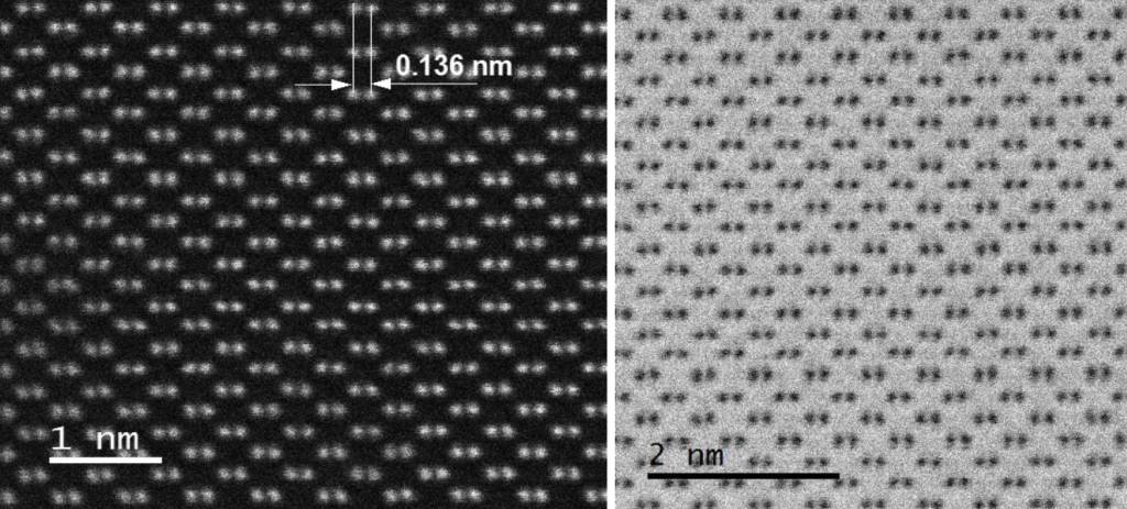
HAADF STEM and BF STEM images of single crystal Si oriented in [110] direction. Bright/dark spots are columns of Si atoms captured by HAADF/BF detectors.
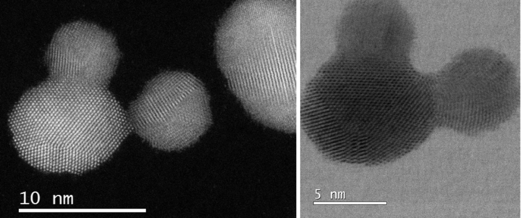
STEM HAADF and STEM BF of Au nanoparticles HRTEM
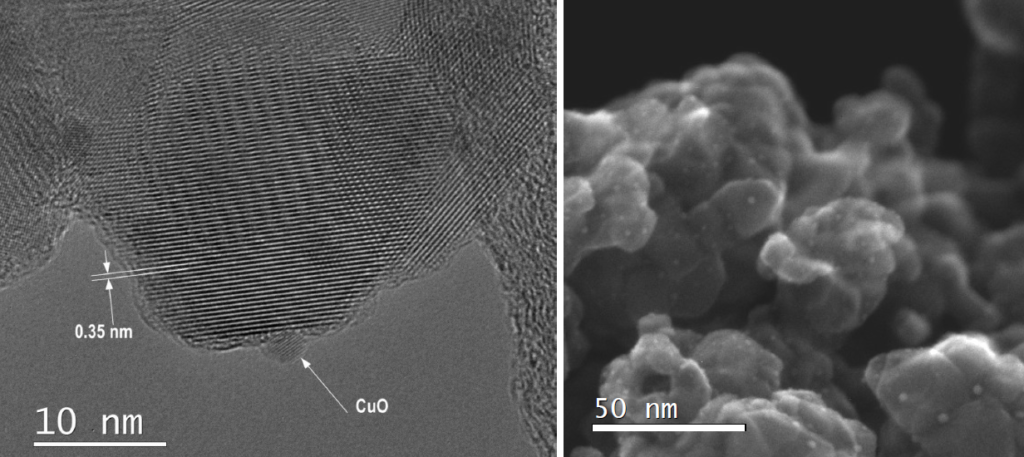
HRTEM and SEI images of nanocomposite anatase TiO2 –CuO sample: Plesch, FNS UK
HAADF image of nanocomposite anatase TiO2 –CuO sample: Plesch, FNS UK
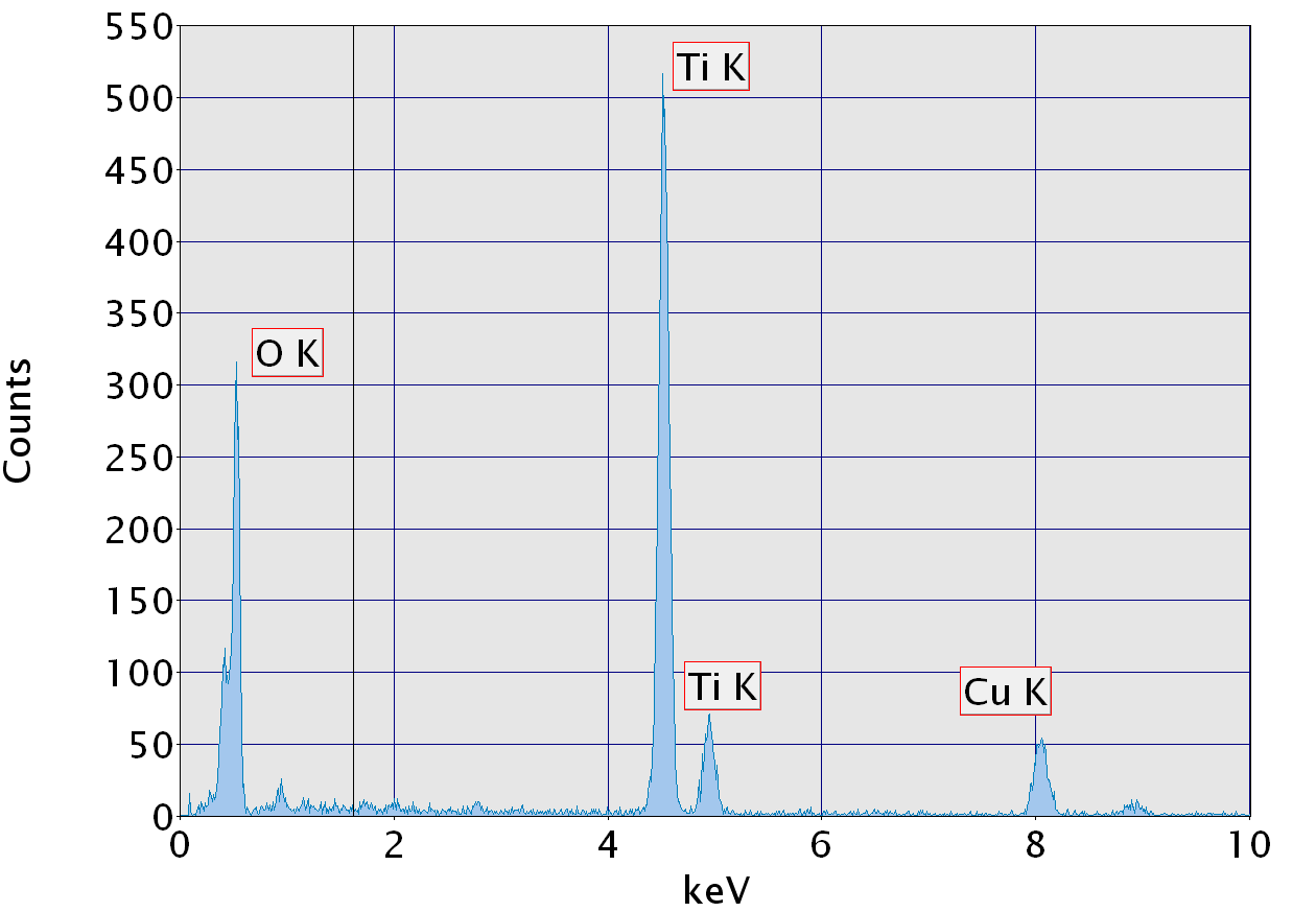
EDS spectroscopy of Anatase –CuO nanocomposite
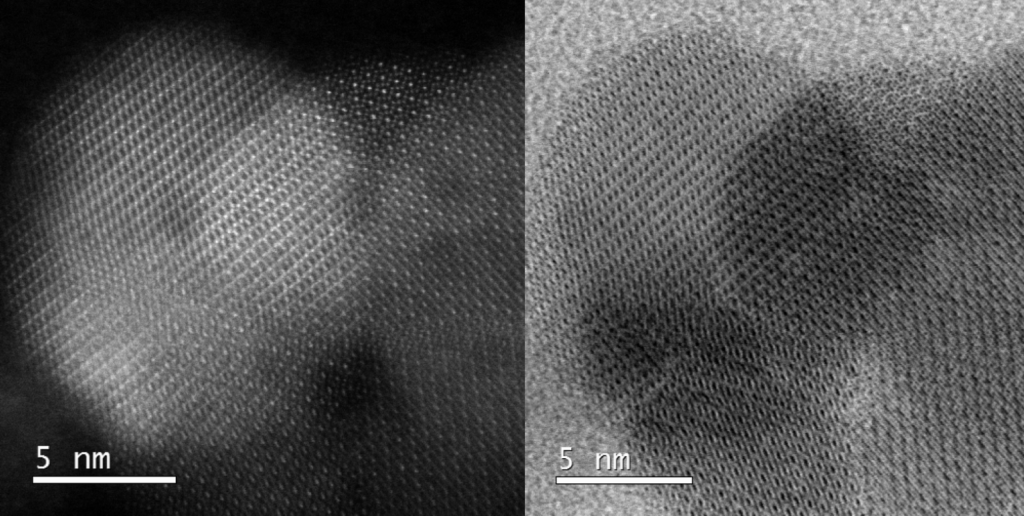
Magnetite (Fe3O4) nanoparticles HAADF and BF STEM images. sample: Kišš, CHTF STU
STEM BF and EDS maps of As, Zn , S from mixture of As4S4(1) –ZnS(4) (sample: Baláž & Co., Institute of Geotechnics, SAS, Košice)
Nanoparticles are agglomerated into densely packed irregular aggregates. EDX maps of As L and Zn K are presented. The overlay of these images visualizes the local changes in Zn (red) and As (green) distribution at nanometer scale. The yellow color represents the areas where both As and Zn coexists.
HAADF STEM and BF STEM images and atomic EDS maps of GaAs single crystal oriented in [110] direction. As, Ga EDS maps and overlay image. As, Ga, and overlay, Atomic mapping using EDS
Jeol JEM ARM 200cF parameters:
| Illumination system | |
| Type of electron gun: | cold field emission, tungsten emitter |
| Acceleration voltage: | 200 kV, 80 kV, preparation for 60 kV |
| Energy FWHM: | 0.3 keV at 200 kV |
| Brightness: | 8 × 10⁻⁸ A /cm2 srad at 200 kV |
| Probe current: | 5 × 10⁻¹⁰ A |
| STEM corrector: | built-in |
| TEM corrector: | built-in |
| Achieved resolution | |
| TEM resolution (point-to-point): | 114 pm |
| TEM resolution (lattice): | 56 pm |
| TEM magnification: | 50 ̶ 2,000,000 × |
| STEM resolution – dark field (HAADF): | 76 pm |
| STEM resolution – bright field: | 96 pm |
| STEM magnification: | 200 ̶ 150,000,000 × |
| STEM resolution (backscattered electrons): | 0.63 nm |
In STEM mode, following detectors are available: ABF (annular bright field), LAADF (low-angle annular dark field), HAADF (high angle annular dark field).
| EDS detector | |
| Detector type: | silicon drift detector |
| Effective area: | 100 mm2 |
| Resolution (Mn Kα line): | 127 eV |
| Collection angle: | 0.98 srad |
| EELS detector | |
| Detector type: | GATAN imaging filter |
| Zero loss peak FWHM at (pri 0.1 µA): | 0.29 eV |
| Resolution (at 1 µA): | 0.32 eV |
| Resolution (at 10 µA): | 0.45 eV |
