Laboratory of Transmission Electron Microscopy
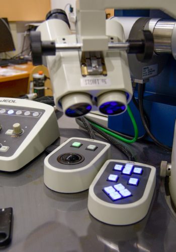
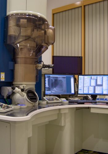
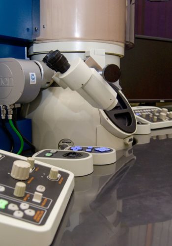
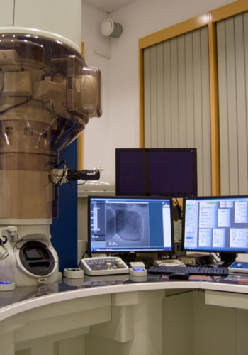
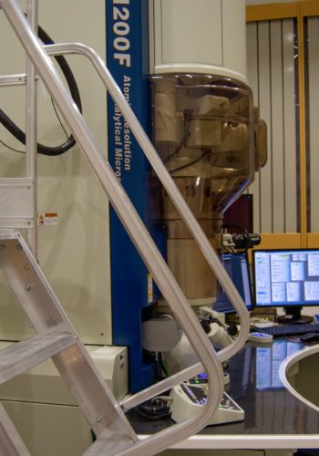
Analytical transmission electron microscope Jeol JEM ARM 200cF with the resolution of 0.78 Å equipped with field auto emission electron source and with two correctors of spherical aberration enables a complex characterization of nanostructured objects on the subatomic level by the means of the following methods: imaging with high angle annular dark field detector (HAADF), imaging with low angle annular dark field detector (LAADF), imaging with annular bright field detector (ABF) in scanning regime (STEM), in TEM/HRTEM regimes, and imaging in backscattered electron (BEI) and secondary electron regimes (SEI). Electron diffraction methods (selected area diffraction, nanobeam diffraction, convergent and precession diffraction) are available to acquire the information related to crystallographic structure. Further possibilities include orientation and phase mapping, qualitative and quantitative energy dispersive analysis (EDS), electron energy loss spectroscopy (EELS) and mapping of atom distribution in the sample. Microscope has incorporated Lorentz mode for characterisation of magnetic samples and biprism for electron holography. 3D morfology of nanoscaled objects can be obtained by employing electron tomography. Other adjacent laboratories serve for preparation of TEM samples where various physical and chemical methods are exploited.
Installed: 2015
more… Laboratory of Atomic Resolution Transmission Electron Microscopy
Laboratory of Auger Spectrometry
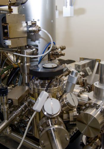
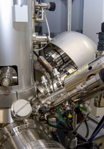
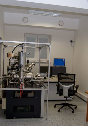
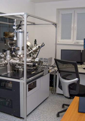
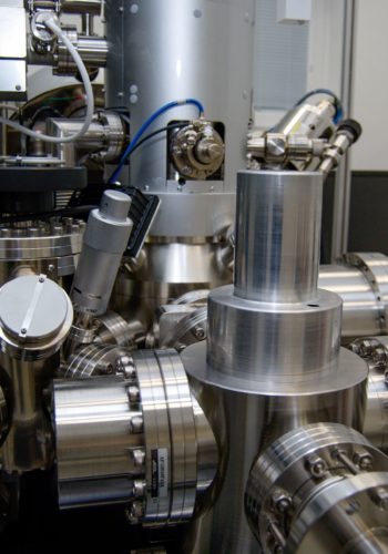
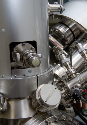
The laboratory is equipped with Auger electron microprobe Jeol JAMP-9510F with Schottky electron gun. The device desirably combines electron microscopy and Auger spectrometry. The resolution in secondary electron mode is 3 nm, the diameter of the electron beam during Auger electron analysis is 8 nm. The device enables to acquire information about elemental composition from few atomic layers to nanometres of depth of sample under study (with some overreach into chemical analysis). Also, Auger maps, Auger depth profiles and electron loss spectra can be acquired. The best energetic resolution ΔE/E is 0.05 %. Bulk samples can be fractured directly in a vacuum chamber to reduce surface contamination.
Installed: 2015
FIB-SEM Laboratory
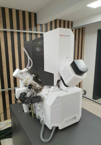
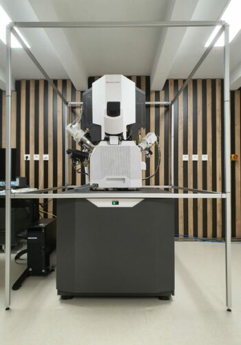
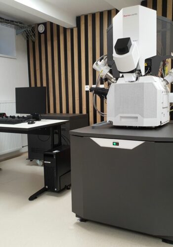
The Thermo Scientific Scios 2 DualBeam System is a high-resolution scanning electron microscope (SEM) equipped with a focused ion beam (FIB) for sample patterning and nanomachining. The system is equipped with several detectors for complex sample observation and analysis. The microscope can operate in a low vacuum regime which is better suited for nonconductive samples. A focused ion beam together with a nanomanipulator and GIS system makes the device suitable for preparation of TEM samples.
Installed: 2022
more… FIB-SEM Laboratory
Laboratory for sample preparation
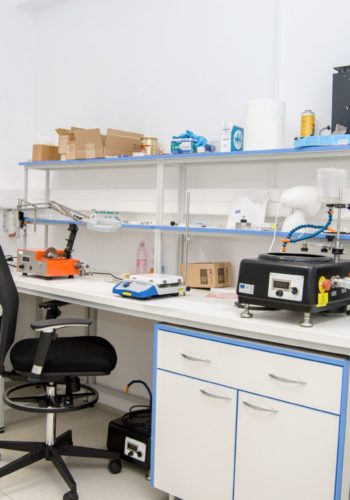
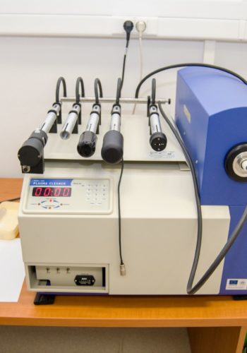
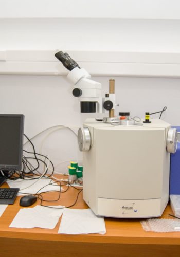
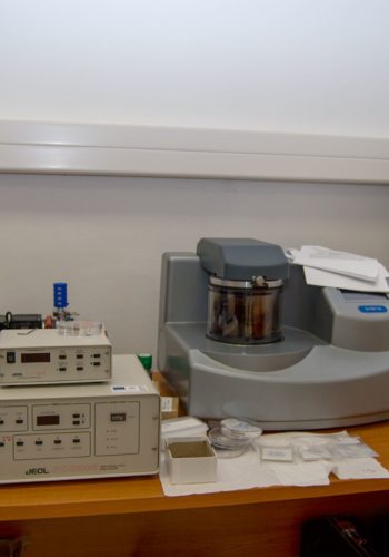
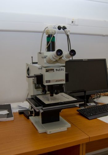
Wide span of possibilities is accessible for sample preparation including vacuum depositions (vacuum evaporation, vacuum sputtering), mechanical preparation (grinding, polishing, ultrasonic cutting, diamond saw cutting), ion technologies (ion thinning, plasma cleaning) and chemical preparation (electrochemical thinning, etching).

