
Outline of the method
Auger electron spectroscopy (AES) is a method of elemental identification. A sample under study is irradiated by electron beam (or X-ray quantum) to generate secondary electrons, among which so called Auger electrons are the subject of interest. Auger electrons carry unique information about composition of the sample under study correlated to their energy. By measuring electron spectra we can extract the composition because each element of the periodic table has its own typical energies of Auger transitions which can be find in tables and atlases. AES is cable to analyze the elements in the periodic table starting with Li. The sensitivity of the methods is practically somewhere around 0.5 at.% and varies from element to element.

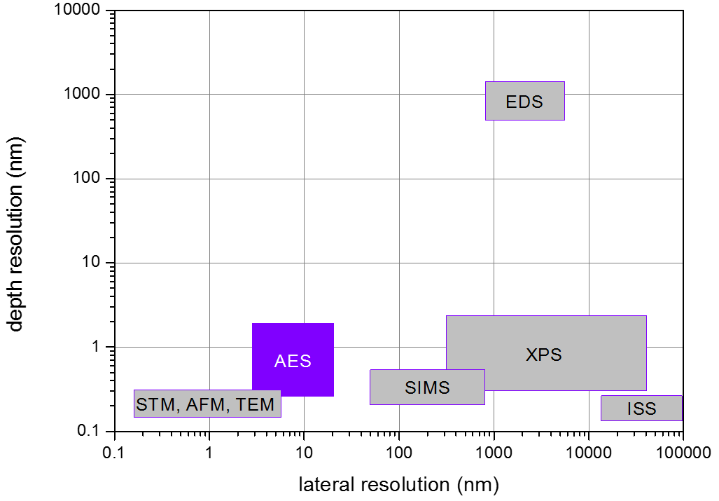
There are four main advantages of AES over energy-dispersive spectroscopy (EDS):
- Information depth of Auger electrons varies in dependence on the examined element and is in the range 1 – 10 nm. Therefore, AES is truly surface method, which overwhelms EDS significantly (information depth is in order of microns).
- Auger yield is bigger for light elements which can cause difficulties (in terms of low signal) when examined with EDS since EDS is more suitable for heavier elements.
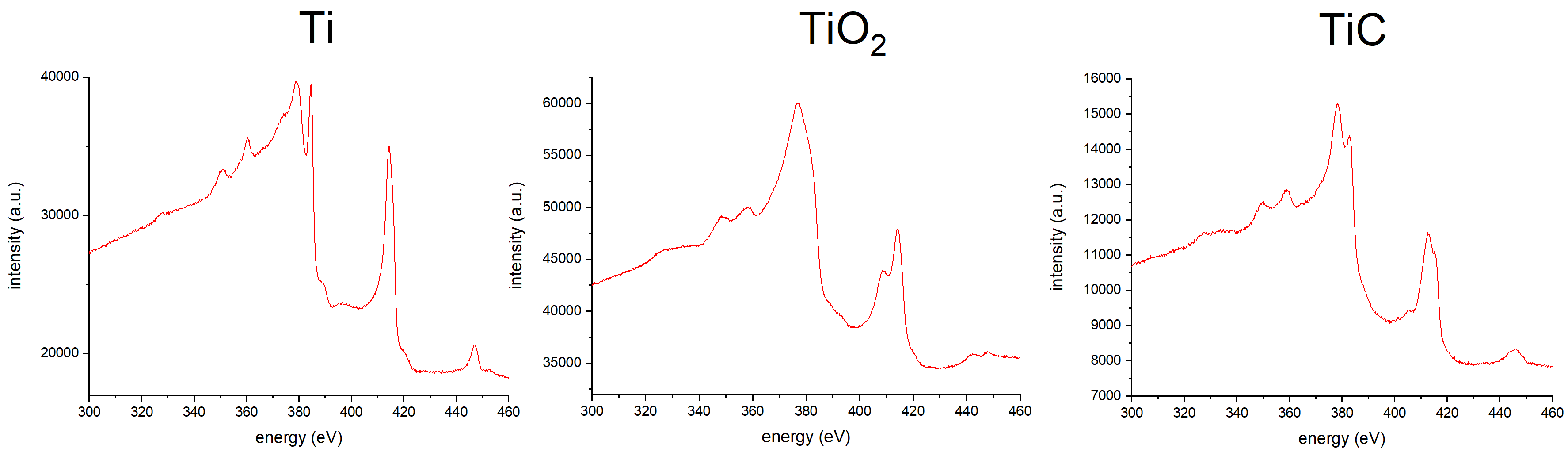
- The presence of chemical bond affects the shape of Auger electron spectra, so chemical analysis is possible to some extent.
- In the case of monolayer coverage or even sub-monolayer coverage AES is effective technique
Quantitative AES
AES is commonly used as a quantitative technique. Traditional approach for quantitative AES is via relative sensitivity factors, a simple method which works well in many cases. But the most reliable method is examination of standard sample. Composition of standard sample may be determined by EDS.
Possible fields of application
Typical applications of AES can be found in semiconductors, metallurgy, steel failure, welding, thin films and coatings, multilayers and optical layers, soldering, corrosion, oxidation, tribology. Nanostructures belong to specific area, very suitable for investigation via AES.
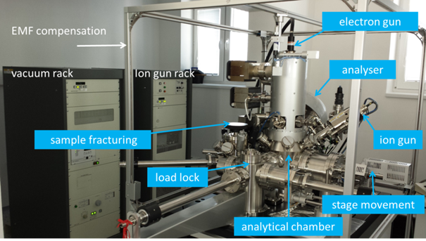
Our device
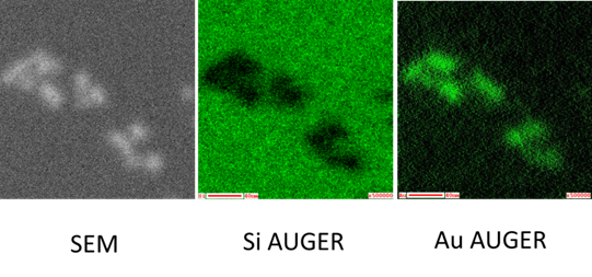
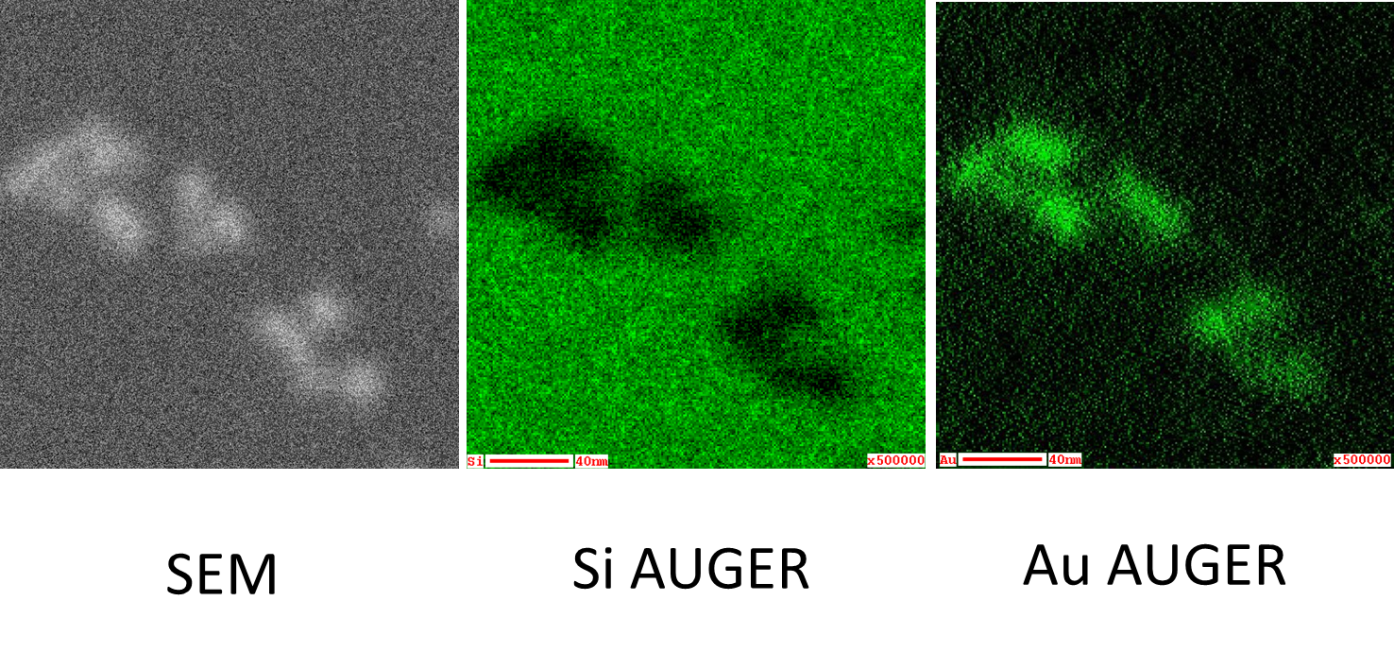
The installed deviced is Auger microprobe JEOL JAMP 9510-F combining the advantages of scanning electron microscopy and Auger electron spectroscopy. Electron imaging can be directly correlated with Auger maps. In secondary electron imaging, the best resolution is 3 nm and the smallest spot of the electron beam in the Auger analysis mode is 8 nm. Owing to these parameters, the device is dedicated to analysis of nanostructures. Possible operating modes:
- Secondary electron imaging
- Backscattered electron imaging (topography or composition mode)
- Recording of Auger spectra in spot / area mode (direct or differentiated spectra)
- Auger line profile
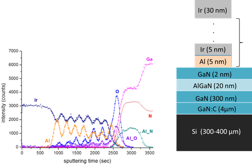
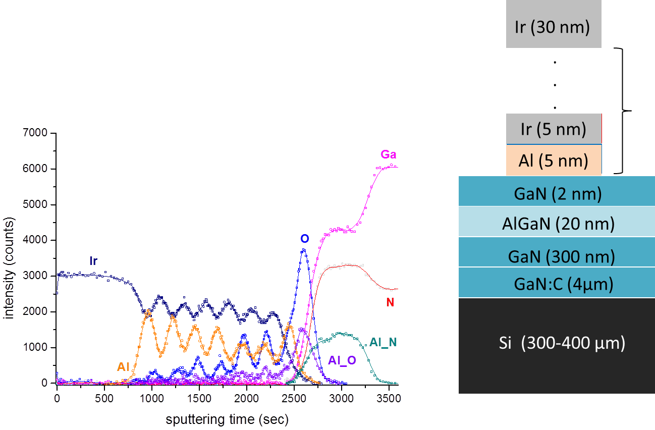
- Auger depth profiling (using 0.5 – 3 keV Ar+ ion beam for sputtering)
- Auger imaging
- Chemical analysis in reasonable cases
- Recording / imaging of plasmon excitation
Sample requirements
- Vacuum compatibility (10-7 Pa)
- Durability under e– beam (0.5 – 30 keV, 10 nA)
- Max. sample thickness for depth profiling <1000 nm
- Electrical conductivity (e.g. thermal or CVD SiO2 is relatively conductive)
Typical size of the samples:
- Circular sample: φ = 20 mm in diameter or less, 10 mm is better.
- Special holder: the diameter of hard disk
- Rectangular sample: max. 14 × 14 mm
- We have also a fracturing device which serves for sample fracturing at liquid nitrogen temperature. This is done directly in the analytical chamber so we can avoid contamination. Type a message for more info.