
PROJECT
Auger electron spectroscopy for surface studies of two-dimensional MoS2 layers
ABSTRACT
In recent decades, a huge effort has been paid to the research of various 2D layers including MoS2. Their applicability to broad range of problems, including environmental and climate issues, still attracts the scientists in various fields. But due to technological challenges connected with the production of cleaner 2D surfaces, their application potential has not been fulfilled yet. The aim of the project is to determine how the contamination affects the surface composition of supported and suspended MoS2 layers and how it changes with the applied cleaning procedures. As the tool for the study, Auger electron spectroscopy (AES) will be employed, promoting itself as an exceptional analytical method for 2D layersaddressing the problems of local surface composition, contamination, homogeneity, and cleaning. Response of electrons in MoS2 surfaces to primary electrons will be studied as well, with expected interesting effects not yet described in the methodology of AES.
PROJECT DETAILS
Project number: 09I03-03-V04-00457
Framework/Call: 09I03-03-V04 – Scholarships for Excellent Researchers
Component: Component 9 – More efficient management and strengthening of funding for research, development, and innovation.
Investment: Investment 3 – Excellent Science
Funder: European Union (NextGenerationEU)
Duration: 01 September 2024−31 August 2026
PUBLICATIONS
Ľubomír Vančo, Ravi K. Biroju, Mário Kotlár, Viliam Vretenár, Dipak Maity, Tharangattu N. Narayanan
Nondestructive Imaging and Quantification of Composition in 2D MoS2 and V-Dpoed MoS2 by the Auger Scatterplot Method
In: J. Phys. Chem. C 2025, 129, 20995−21004, https://doi.org/10.1021/acs.jpcc.5c05299
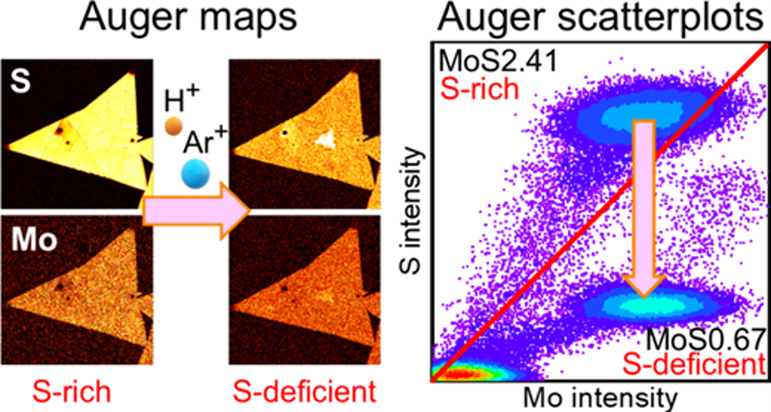
Molybdenum disulfide (MoS2) monolayers have emerged as promising materials for a variety of applications. Their behavior depends critically on surface composition; therefore, careful characterization is necessary to describe their properties accurately. Although Auger electron spectroscopy (AES) is a standard method capable of addressing this issue, it suffers from beam-induced damage and variation of spectral features in complex samples. To overcome these limitations, we employed correlative analysis to examine MoS2 and V-doped MoS2 2D surfaces by using Auger scatterplots. As we demonstrate, this method enables the nondestructive imaging and assessment of the lateral and depth distributions of the elements and provides a remarkably convenient way to estimate S-rich/depleted regions. The scatterplot technique indicates that V doping in MoS2 retards desulfurization in an Ar/H2 plasma environment. By reducing the electron dose, the analysis using scatterplots can improve the accuracy of AES by up to 30%. The Auger scatterplot method provides insight into the affinity or independence of surface constituents through quantitative relationships, enabling separate analysis of the characteristic areas within a complex sample. These findings are supported by Raman spectroscopy and transmission electron microscopy, which highlight the effectiveness of the Auger scatterplots and their potential for examining the surfaces of 2D materials. Auger maps also show a strong correlation with photoluminescence features in MoS2 monolayers, thereby illustrating the overlap with practical applications.
Other publications:
Ľubomír Vančo, Ravi K. Biroju, Mário Kotlár, Viliam Vretenár, Dipak Maity, Tharangattu N. Narayanan: Analysis of two-dimensional molybdenum disulfide layers by scanning Auger microscopy. In: Extended Abstract Book of 14th Conference “Solid State Surfaces and Interfaces” November 18-20, Smolenice, Slovak republic, Comenius University, ISBN 978-80-223-5941-2.
Ľ. Vančo, M. Kotlár, P. Vogrinčič, M. Štrbák, S. Dharmapuri, Determination of thickness in suspended MoS2 layers using backgrounds in Auger electron spectra. In: Proceedings of ADEPT – the International Conference on Advances in Electronic and Photonic Technologies, Nový Smokovec, Slovakia, june 15th – 18th, 2026, EDIS-Publishing Centre of UNIZA, ISBN 978-80-554-2303-6.