Rok: 2025

In-situ CVD Grown WS2-MoS2 Lateral Heterostructure with Alloyed Interface: Strong Photoluminescence Enhancement and High On-Off Ratio Field Effect Transistors

Abdul Kaium Mia, Sourav Dey, Lubomir Vanco, Viliam Vretenar, P. K. Giri

In: Materials Today Nano 31, 100638 (2025)

https://doi.org/10.1016/j.mtnano.2025.100638

Abstract:

The semiconducting 2D transition metal dichalcogenides (TMDs) have gained substantial attention, though the progress in their lateral heterostructures (HS) and in-situ growth for electronic and optoelectronic applications has been very limited. Herein, we report a single-step in-situ chemical vapor deposition growth of bilayer WS2-MoS2 lateral HS, which ensures a clean diffused interface between WS2 and MoS2, enabling efficient charge transport. The spatial Raman, photoluminescent (PL), and Auger mapping of in-situ WS2-MoS2 lateral HS shows a clear transition from pure WS2 to pure MoS2 region through a graded WS(1-x)MoxS2 alloy interface. The composition and the width of the alloy interface could be tuned by careful choice of the proportion of precursor materials and by tuning the growth parameters. Spatially resolved PL spectra and PL mapping reveal a strongly enhanced (more than one order of magnitude) PL intensity in the HS interface attributed to the strain-induced bandstructure modification in the alloyed interface. Interestingly, the alloyed interface in the lateral HS also dramatically improves the electronic properties, resulting in an on-off ratio of 108 in the fabricated field effect transistor, which is two orders of magnitude higher than their individual counterpart. These results on lateral HS are significant, and they pave the way to synthesize other different HSs for future electronic devices and integrated circuits.

Valley Engineering of Monolayer MoS2 via Substitutional Cr and V Dopants and the Mechanistic Insights

Valley Engineering of Monolayer MoS2 via Substitutional Cr and V Dopants and the Mechanistic Insights

Sreekant Anil, Dipak Maity, Snehith Adabala, Arpan De, Nagendra S. Kamath, Raheel Hammad, Janmey Jay Panda, Ravi K. Biroju, Viliam Vretenar, Rajalakshmi G, Suman Kalyan Pal, Soumya Ghosh, and Tharangattu N. Narayanan

In: Nano Lett. 2025

https://doi.org/10.1021/acs.nanolett.5c03877

Abstract:

MoS2 monolayers (MS) having magnetic impurities as dopants can bring about time-reversal asymmetry and hence room temperature magnetism. Here, we demonstrated the synthesis of Cr substitutionally doped (∼1%) MS (CrMS) along with its vanadium-doped MS counterpart (VMS) and investigated their suitability for valleytronics by studies based on chirality-selective photoluminescence, time-resolved transient absorption spectroscopy, and spin Hall effect of light (SHEL). While VMS showed room temperature valley splitting, no such shift was observed in CrMS although with their expected similarity. Density-functional-theory-based electronic structure calculations indicate a Cr-induced flat band below the Fermi level, even at ∼0.5 atom % doping, which masks the splitting in the energies of the K-point valleys. This finding is in tune with the experimental studies while in contrast to the theoretical and experimental data of VMS. Hence, this study establishes band valley tunabilities of MoS2, and SHEL as a powerful tool for valley polarization studies.

Titulná strana v ACS Applied Electronic Materials

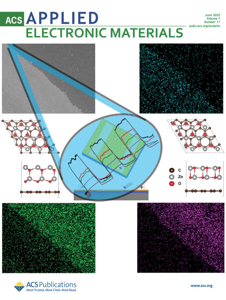
Publikácia Graphene-ZnO Thin-Film Heterostructure-Based Efficient UV Photosensors, na ktorej sme sa autorsky podieľali, bola nedávno umiestnená na titulnú stranu časopisu ACS Applied Electronic Materials . Dr. Ravi K. Biroju, hlavný autor publikácie, vysvetľuje, že daná práca demonštruje prípravu van der Waalsovej heteroštruktúry grafén/ZnO v podobe tenkej vrstvy metódou CVD. Ak skombinujeme priamy polovodičový materiál s veľkou šírkou zakázaného pásma ako ZnO a vodivú vrstvu grafénu, dostaneme platformu s možnosťami jej aplikácie v oblasti fotosenzorov, alebo plynových senzorov. V prípade osvetlenia danej štruktúry dôjde k efektívnej separácii svetlom generovaných elektrón-dierových párov lokálnym elektrickým poľom, čo efektívne potlačí ich rekombináciu a zvýši životnosť nosičov náboja. Výsledkom je k zvýšenie hustoty nosičov náboja. Ďalej to vedie k zníženiu Schottkyho bariéry medzi tenkou vrstvou ZnO a grafénom, čo zlepšuje transport nosičov náboja. Výsledkom je vysoký pomer prúdov osvetlenej a neosvetlenej štruktúry Ilight/Idark , oveľa väčší než pre samotné tenké vrstvy, alebo nanoštruktúry ZnO.

Graphene-ZnO Thin-Film Heterostructure-Based Efficient UV Photosensors

Graphene-ZnO Thin-Film Heterostructure-Based Efficient UV Photosensors

Ravi K. Biroju*, Sanat Nalini Paltasingh, Mihir Ranjan Sahoo, Soumen Dhara, Dipak Maity, Viliam Vretenár, P. K. Giri, Tharangattu N. Narayanan, Saroj Kumar Nayak

In: ACS Applied Electronic Materials

https://doi.org/10.1021/acsaelm.5c00348

Abstract

Graphene-based ZnO thin-film hybrids (GR-ZnO) have shown interesting properties for electronic and optoelectronic applications, such as enhanced UV photodetection and photocatalysis. The interaction and explicit role of large-area single-layer chemical vapor deposition (CVD)-grown graphene in the improved photophysical properties in such a kind of GR-ZnO hybrids have not been well-understood in recent reports. In the present work, we fabricated a photosensor made with large-area monolayer CVD GR-ZnO thin-film hybrids, which showed improved UV photodetection with high values of UV sensitivity and responsivity compared to bare ZnO films. The GR-ZnO thin-film hybrid photosensors demonstrated about a 20 time improvement in photoresponsivity (9.87 × 10³ A/W) compared to the bare ZnO thin film (4.93 × 10² A/W). We investigated the origin of the high photosensitivity of GR-ZnO, and it is explained based on a comparatively large absorption coefficient, enhancement of the number of photogenerated carriers, and a reduction of the recombination rates of these carriers based on density functional theory (DFT) calculations. The high mobility of the graphene layer provides an efficient and faster charge transfer pathway for photogenerated carriers at the interface between ZnO and the graphene layers.