Autor CND

Large-Scale Direct Growth of Monolayer MoS2 on Patterned Graphene for van der Waals Ultrafast Photoactive Circuits

Rahul Sharma, Henry Nameirakpam, David Muradas Belinchón, Prince Sharma, Ulrich Noumbe, Daria Belotcerkovtceva, Elin Berggren, Viliam Vretenár, Ľubomir Vančo, Matúš Maťko, Ravi K. Biroju, Soumitra Satapathi, Tomas Edvinsson, Andreas Lindblad, M. Venkata Kamalakar*

In: ACS Applied Materials & Interfaces, Vol 16, Issue 29

https://doi.org/10.1021/acsami.4c07028

Abstract

Two-dimensional (2D) van der Waals heterostructures combine the distinct properties of individual 2D materials, resulting in metamaterials, ideal for emergent electronic, optoelectronic, and spintronic phenomena. A significant challenge in harnessing these properties for future hybrid circuits is their large-scale realization and integration into graphene interconnects. In this work, we demonstrate the direct growth of molybdenum disulfide (MoS2) crystals on patterned graphene channels. By enhancing control over vapor transport through a confined space chemical vapor deposition growth technique, we achieve the preferential deposition of monolayer MoS2 crystals on monolayer graphene. Atomic resolution scanning transmission electron microscopy reveals the high structural integrity of the heterostructures. Through in-depth spectroscopic characterization, we unveil charge transfer in Graphene/MoS2, with MoS2 introducing p-type doping to graphene, as confirmed by our electrical measurements. Photoconductivity characterization shows that photoactive regions can be locally created in graphene channels covered by MoS2 layers. Time-resolved ultrafast transient absorption (TA) spectroscopy reveals accelerated charge decay kinetics in Graphene/MoS2 heterostructures compared to standalone MoS2 and upconversion for below band gap excitation conditions. Our proof-of-concept results pave the way for the direct growth of van der Waals heterostructure circuits with significant implications for ultrafast photoactive nanoelectronics and optospintronic applications.

Quantification of alloy atomic composition sites in 2D ternary MoS2(1-x)Se2x and their role in persistent photoconductivity, enhanced photoresponse and photo-electrocatalysis

Ravi K. Biroju, Dipak Maity, Viliam Vretenár, Ľubomír Vančo, Rahul Sharma, Mihir Ranjan Sahoo, Jitendra Kumar, G. Gayathri, Tharangattu N. Narayanan, Saroj Kumar Nayak

In: Materials Today Advances, Volume 22, 2024, 100504

https://doi.org/10.1016/j.mtadv.2024.100504

Abstract

Engineering transition metal dichalcogenides-based semiconducting two-dimensional (2D) layered materials for photo(electro)chemical (PEC) hydrogen evolution reaction (HER) by water splitting is an enduring challenge. Here, alloy-assisted photoconductivity and photoresponse from CVD-grown MoS2(1-x)Se2x (MSSE) 2D ternary atomic layered alloy-based photodetector device is presented for the realization of PEC HER. The explicit role of ‘S–Se’ and ‘Se2’ atomic alloy sites including chalcogen-induced vacancy defects on the photoconductivity/photoresponse and PEC HER performance of MSSE 2D alloy is investigated. Alloy formation, atomic site-by-site ‘Se’ composition and atomic structure are characterized using Raman/Photoluminescence (PL) spectroscopy, high-angle annular dark field (HAADF)- scanning transmission electron microscopy (STEM) extensively and supported with Auger Electron Spectroscopy (AES) mapping. Further, the local density and concentration of S–Se, Se2 atomic sites and defects were quantitatively estimated using HAADF-STEM image analysis in correlation with AES and it is found between the range of ∼15–20 % in MSSE alloy. A 10-fold high photoresponsivity in the case of MSSE concerning as-grown MS having fast photocurrent growth time and the prolonged decay time originates from the ‘Se’ and this alloy assisted states to enhance the PEC performance of MSSE alloy. The enhanced PEC HER activity of MSSE alloy was identified in terms of overpotential and current density. In addition, increased density of states as a function of ‘Se’ alloying, shifts in a p-band centre and lowers ΔGH* according to density functional theory calculations, which makes MSSE alloy an efficient HER activity. Further, the PEC stability and presence of the ‘S–Se’ and ‘Se2’ alloying and their role towards HER have been correlated by the spectral line shape analysis of PL and Raman spectra from post-PEC HER catalysts. These experimental and theoretical findings establish the role of chalcogen, and transition metal-based 2D alloy, leading to the design of new PECs of engineered 2D atomic layer interfaces.

Inštalácia FIB-SEM mikroskopu

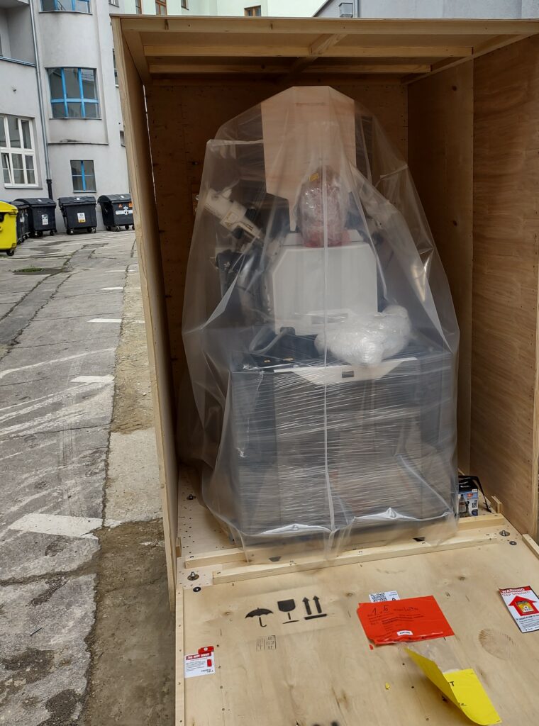
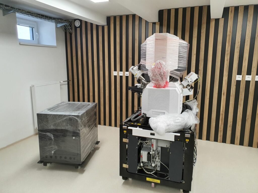
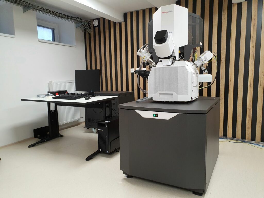
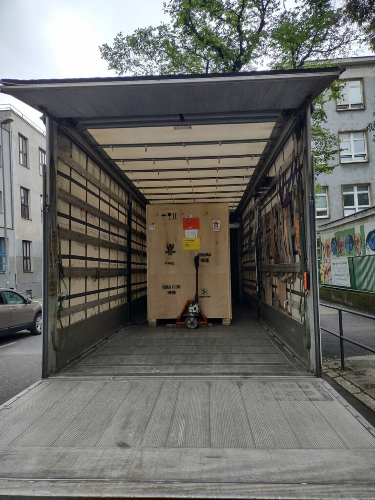
Začiatkom Júna sa v priestoroch Centra pre Nanodiagnostiku Materiálov, ktoré patrí pod MTF Trnava, začala inštalácia nového FIB-SEM mikroskopu. Zariadenie bolo privezené z výrobného závodu firmy Thermo Fisher Scientific (bývalá firma FEI) v Brne do Bratislavy, kde bolo inštalované v novo zrekonštruovaných priestoroch Centra. Po náročnom transporte zariadenia do suterénu, bol mikroskop úspešne zostavený a spustený. Po následnej sérii nastavení, kalibrácií a testov bol mikroskop odskúšaný a uvedený do prevádzky. Keďže mikroskop spĺňa požadované parametre, môžeme konštatovať, že mikroskop je pripravený splniť všetky náročné požiadavky, ktoré sú naň kladené.

Mikroskop dorazil do Bratislavy
Inštalácia
Covalent Diamond–Graphite Bonding: Mechanism of Catalytic Transformation

Covalent Diamond–Graphite Bonding: Mechanism of Catalytic Transformation

Semir Tulić, Thomas Waitz, Mária Čaplovičová, Gerlinde Habler, Marián Varga, Mário Kotlár, Viliam Vretenár, Oleksandr Romanyuk, Alexander Kromka, Bohuslav Rezek, Viera Skákalová

ACS Nano, 2019, 1344621-4630

https://doi.org/10.1021/acsnano.9b00692

Abstract

Aberration-corrected transmission electron microscopy of the atomic structure of diamond–graphite interface after Ni-induced catalytic transformation reveals graphitic planes bound covalently to the diamond in the upright orientation. The covalent attachment, together with a significant volume expansion of graphite transformed from diamond, gives rise to uniaxial stress that is released through plastic deformation. We propose a comprehensive model explaining the Ni-mediated transformation of diamond to graphite and covalent bonding at the interface as well as the mechanism of relaxation of uniaxial stress. We also explain the mechanism of electrical transport through the graphitized surface of diamond. The result may thus provide a foundation for the catalytically driven formation of graphene–diamond nanodevices.